Hello, my name is Bob Willis and welcome to Defect of the Month with WNIE TV. Here is another video to watch. Pin In Hole Intrusive Reflow is covered this month with a short, illustrated article to add to your collection of training material. Hopefully with my FREE eBook on Intrusive Reflow Design & Assembly it will help your team understand process and product failures.
Pin in hole, intrusive, multi spot soldering, there are lots of terms used for this method of soldering based on location around the world. Basically its soldering through hole components, solder paste in plated through holes and making reliable connections. First thing you can do is download a copy of my FREE eBook. I wrote this book a couple of years back covering all aspects of the process and my practical experienced over the years running this process. If you’d like a copy all you need to do is, ask. In my opinion it’s a very simple process, it works, and we have lots of evidence to demonstrate the reliability of the solder joints produced.
So let’s just step back for a second rather than talk about the process because you can read the book but talk about some of the issues like damage to components. If select components that won’t stand up to the reflow soldering process, be it vapour phase or convection reflow that’s a design related issue. The design engineer needs to make sure components are compatible with peak temperature of the reflow process. Using popular low temperature solder alloys make it even easier. If you are going to be using multiple or alternative suppliers of components peak temperature needs to be understood.
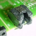
Above are just a couple component examples that have been damaged and obviously won’t work very successfully, the quality guys will not like them either
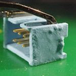
The next issue I tend to find is poor solder fill, but a lot of that is due to the hole to lead ratio. If you have a large hole and a small pin, you’ve got to put a lot more paste into the hole and on the surface of the pad. What we’re trying to do is get the process properly balanced. If you go by my very simple design rule, the finished hole size should be 10 thousands of one inch greater than the maximum pin size. If it’s a round pin, it’s straightforward to measure. If it’s a square pin or an oblong, it’s measured across the largest corner, it’s that simple.
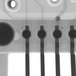
Examples of different solder fill after intrusive reflow
I have found over the years that I can use components and boards using these simple design rules with automatic SMT assembly. So you may be able to use your placement machine if it’s capable of working with odd form components, you don’t have to assemble it all manually. Follow this and you should achieve IPC Level 3 minimum standards easily for through hole fill. I’ve used intrusive reflow on high temperature, normal lead free and low temperature solder alloys. I can tell you based on results that we’ve achieved very successful and reliable results based on mechanical and environmental testing.
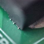
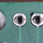
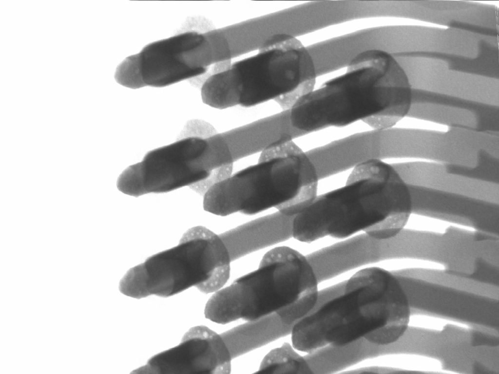
Examples of the solder beads or balls formed after reflow soldering. Mainly due to the
body or connector standoff points contacting the paste.
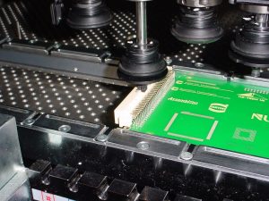
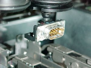
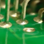
Component insertion using SMT placement equipment on Bobs Test Board
Solder balls or beads are generally caused by solder paste being displaced underneath the component body during the connector or socket insertion process. The stencil design aperture may need to be verified, with these components you can’t do it in isolation. You can work out the volume of solder paste you want, but you’ve got to look at the connector footprint and see the standoff positions of the component body to eliminate solder balls or beads. Remember if you want to use multiple suppliers, they are not all the same!!!
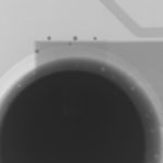
Outgassing and voids, now you’ve heard me talk about printed circuit boards outgassing many times. I have demonstrated my oil test, which is a classic way of demonstrating this particular phenomena of moisture outgassing, but with intrusive reflow. If you have boards that are out gassing when the solder paste goes into its liquid phase and starts to reflow in the plated through hole you may have voids. You can get solder balls spat out from the holes. Now you shouldn’t see this in a good quality printed circuit board today, but it’s worth bearing in mind it’s not the only reason for solder balls.
Outgassing from the PC will create voids but so will poorly defined profiles for PIHR
We can have issues of component pin solderability that we’re using in the process, but that’s a pretty standard defect that could be seen on any soldering process.
Now, if you want a copy of my book on intrusive reflow. All you need to do is ask I’d be more than happy to send you a copy bob@bobwillis.co.uk Thank you very much for reading and continuing to support defect of month and I’ll see you next month.
We have many Defect of The Month videos and WNIE Online articles which we hope will help you solve your process and product failures. We have listed a small selection from over 100 plus videos below created over many years with NPL, IPC & WNIE
BGA popcorning
Dendrite formation
Open solder joints
Solder skips
Coating bubbles
Ultrasonic damage
Missing components
Incomplete past print
Component cracking
Tombstone chips
Solder balls
Solder bead formation
Solder shorts
Sulphur corrosion
Crimp connection failures